bulletin | feature story
Increasing demand for lead-free piezoceramic systems and textured ceramics
By A. Murat Avcı, Servet Kızılırmak, and Ender Suvacı
Piezoelectric ceramics are indispensable to our way of life. Their ability to transform electrical energy into mechanical energy (and vice versa) makes these materials useful in many sectors and industrial applications.
These materials track their origin to the year 1880,1 when the phenomenon of piezoelectricity was first discovered by two French brothers, Jacques and Pierre Curie, in crystals of Rochelle salt and quartz (Figure 1). Later, the Curies discovered that electrical fields can result in dimensional changes in piezoelectric materials, an interaction termed the “inverse piezoelectric effect.”
After World War II, as the number of applications for piezoelectricity started to grow, researchers started to investigate polycrystalline formulations. It was then during the 1950s that the well-known lead zirconate titanate (PZT) was first synthesized.
PZT-based piezoelectric materials offered far superior piezoelectric characteristics than other alternatives proposed to that date. This superior performance led PZT to become the most common piezoelectric ceramic in use today, with applications in numerous fields ranging from energy harvesting equipment to consumer electronics.
The piezoceramic market today
Improved manufacturing techniques and an increasing demand for piezoelectric properties in many fields have allowed piezo device usage to expand in the automotive, avionics, energy harvesting, consumer electronics, and defense industries (Figure 2).
Some prevalent commercial lead-based piezoelectric ceramics are Pb, ZrTiO3 (PZT), (1–x)Pb(Mg1/3Nb2/3)O3–xPbTiO3 (PMN-PT), (1–x)Pb(Zn1/3Nb2/3)O3–xPbTiO3 (PZN-PT), and (1–x–y)Pb(In1/2Nb1/2)O3–yPb(Mg1/3Nb2/3)O3–xPbTiO3 (PIN-PMN-PT). These ceramics, which are modified with dopants to endow them with certain properties, can be classified as either “hard” or “soft” piezoelectrics.
Hard piezoelectrics typically exhibit a coercive field of more than 10 kV/cm. This property is achieved through acceptor doping (Fe3+, Al3+ for PZT), which hardens the domain wall movement and gives the ceramics high power applicability. In contrast, soft piezoelectrics rely on donor doping (Ta5+, Nb5+ for PZT), which makes the domain walls more mobile and thus suitable for low power applications. The coercive field in this case is less than 1 kV/cm.
Piezoceramics can also be categorized based on their applications, either resonance or nonresonance (Rödel et al., 2015).2 In resonance mode systems, piezo stacks stretch and pull back at a frequency close to the natural resonance frequency of the system. Large displacements can be obtained in these systems (Huo et al., 2018).3 Nonresonance systems are frequently used in acceleration, shock, and knocking sensors, as well as energy harvesting systems. Both resonance and nonresonance systems are used in different temperature regimes, and the materials must be designed with Curie temperatures and temperature stabilities proper to these application areas.
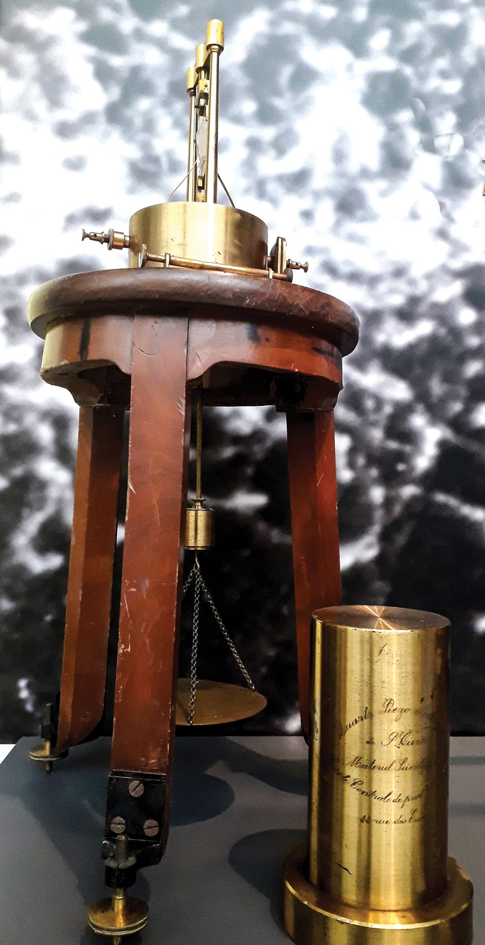
Figure 1. Image of a piezoelectric compensator based on Pierre Curie’s design. It could produce very small electric currents by exerting changing tensile forces on a piezoelectric crystal located near the top of the device.
Credit: Dougsim, Wikimedia (CC BY-SA 4.0)
Figure 1. Image of a piezoelectric compensator based on Pierre Curie’s design. It could produce very small electric currents by exerting changing tensile forces on a piezoelectric crystal located near the top of the device.
Credit: Dougsim, Wikimedia (CC BY-SA 4.0)
ADVERTISEMENT


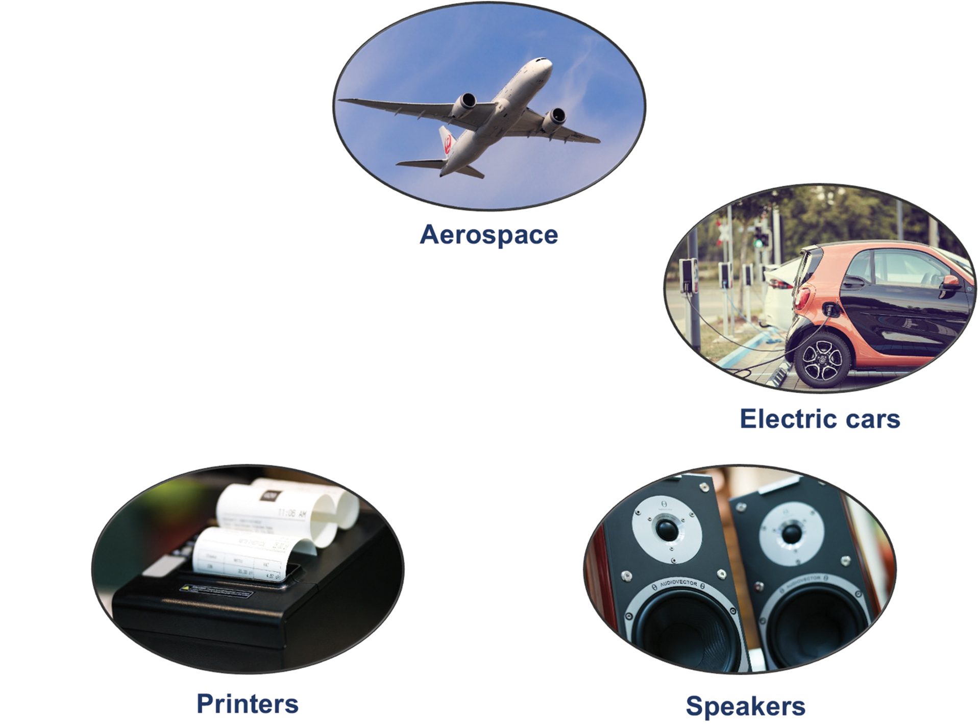
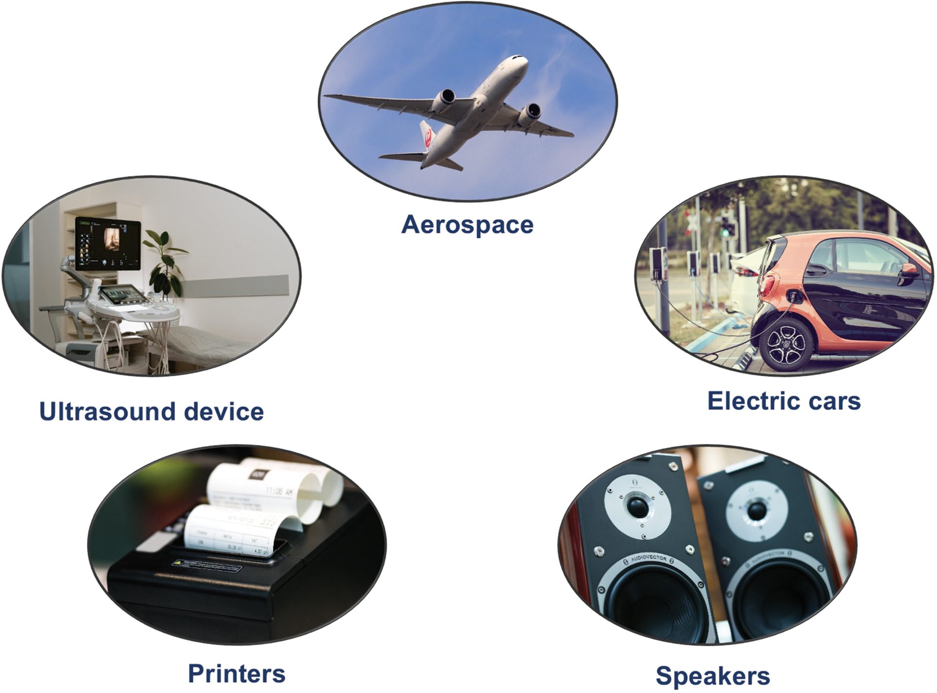
Figure 2. Examples of piezoceramic devices used in daily life.
Credit: All images are in the public domain. Graphic compiled by Entekno.
History of lead-free piezoceramics and the market today
The first studies on lead-free piezoelectric systems took place more than 50 years ago, with the work of Jaeger and Egerton in 1962.7 In 2004, the work of Saito et al. fueled interest in lead-free piezoceramics by showing that the synergistic effect of combining compositional and microstructural design can lead to piezoelectric properties on par with those seen in PZT-based piezoceramics.8 In that study, they doped (Na0.5K0.5)NbO3 with hexagonal pseudo-ilmenite type LiTaO3 to form a morphotropic phase boundary. With this compositional study, improvement in piezoelectricity was supported by hybridization covalency onto ionic bonding by using Cohen’s calculation.9
Investigations into lead-free piezoceramics have concentrated mainly on alkaline niobate (K0.5Na0.5NbO3), barium titanate (BaTiO3), sodium bismuth titanate (Na0.5Bi0.5TiO3), bismuth ferrite (BiFeO3), and their derivates. These piezoceramics are used in the manufacturing, automotive, consumer electronics, and medical sectors, among others. They are used as actuators, sensors, positioning devices, and capacitors, in addition to other applications.
According to a BCC Research report,10 the global market for lead-free piezoelectric ceramics stands at about $184.1 million as of 2021. The market is expected grow to $402.1 million by 2026 at a compound annual growth rate (CAGR) of 16.9%. This projected CAGR for lead-free piezoceramics is greater than the CAGR for the whole piezoelectric market (5.9%).
The increased market penetration of lead-free piezoelectric systems can be directly attributed to stricter environmental regulations worldwide, growing concerns about public health, and expanding demand for piezoelectric devices.

ADVERTISEMENT
Textured piezoceramics
Recently, textured piezoelectric ceramics have attracted attention. These materials exhibit improved properties with respect to conventional piezoceramics, which have randomly oriented grains.
Textured ceramics can be manufactured via a templated grain growth (TGG) process (Figure 3).11 In this process, template particles (anisometric large seeds) are distributed among the fine equiaxed matrix grains. These particles are aligned during the shaping process, and during heat treatment, the templates grow at the cost of fine matrix particles via Ostwald ripening process. Because the particles maintain their initial alignment, the final microstructure is composed of crystallographically oriented grains that exhibit a textured character (Figure 4).
Two important components of the TGG method are the matrix powder and template particles. Matrix powder characteristics should be tailored so that the templates have sufficient thermodynamic driving force to grow at the cost of the fine matrix grains. Additionally, the templates are key components to induce texture development. Template characteristics such as morphology, aspect ratio, thermodynamic stability, and lattice parameter matching with respect to the matrix grains must be carefully considered. Consequently, it is important to form an understanding of the relationship between template characteristics and texture development.
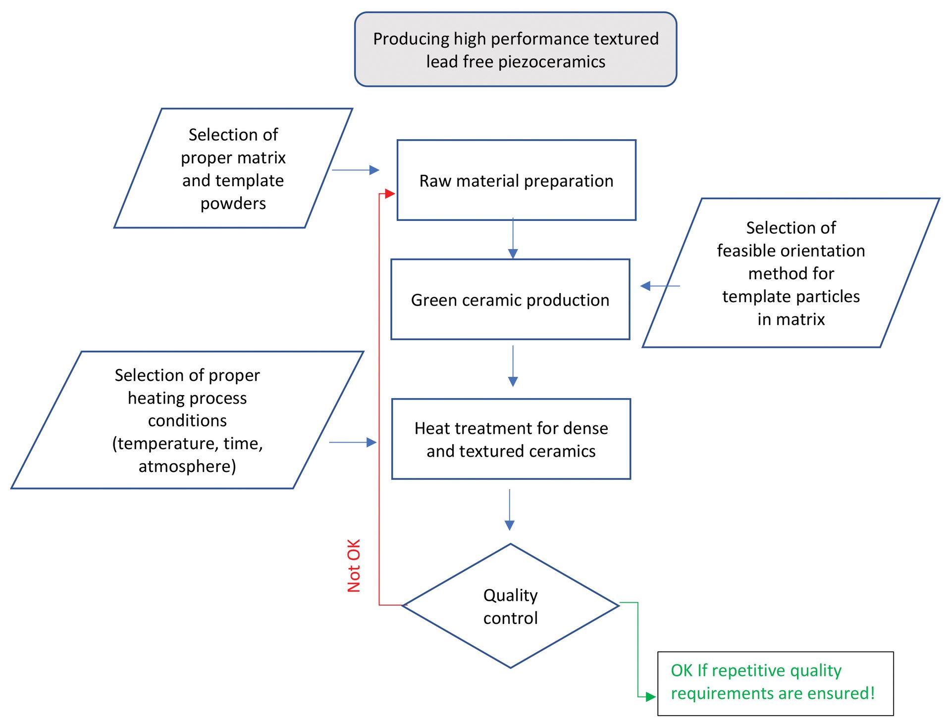
Figure 3. Critical steps of the templated grain growth process.
Credit: Avcı, Kızılırmak, and Suvacı
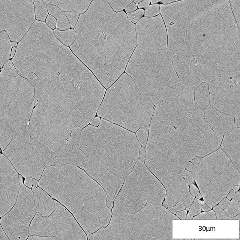
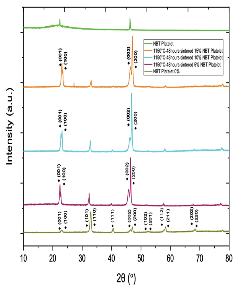
Figure 4. The SEM micrograph (left) and XRD patterns (right) of Na0.5Bi0.5TiO3 platelets and crystallographically textured (Na,K)0.5 Bi0.5TiO3–BaTiO3 system studied by Entekno Materials Co.
Credit: Avcı, Kızılırmak, and Suvacı
Figure 4. The SEM micrograph (above) and XRD patterns (right) of Na0.5Bi0.5TiO3 platelets and crystallographically textured (Na,K)0.5 Bi0.5TiO3–BaTiO3 system studied by Entekno Materials Co.
Credit: Avcı, Kızılırmak, and Suvacı
Figure 4. The SEM micrograph (top) and XRD patterns (bottom) of Na0.5Bi0.5TiO3 platelets and crystallographically textured (Na,K)0.5 Bi0.5TiO3–BaTiO3 system studied by Entekno Materials Co.
Credit: Avcı, Kızılırmak, and Suvacı
Acknowledgements
The authors thank Gamze Welsh for her editorial support during the preparation of this article.
About the authors
A. Murat Avcı, Servet Kızılırmak, and Ender Suvacı are production manager, electroceramic products leader, and chief technology and innovation officer, respectively, at Entekno Materials Co. in Eskişehir, Türkiye. Contact Entekno at info@enteknomaterials.com and visit the website at www.enteknomaterials.com.
SIDEBAR
Driving commercialization of lead-free and textured piezoceramics
Entekno Materials Co. is a leading global materials development company focused on lead-free and textured piezoceramics, headquartered in Eskişehir, Türkiye. Since 2008, Entekno has been an integral materials science innovation partner for piezoelectric manufacturers by providing them with bespoke, high purity, size, and shape controlled dielectric matrix and template particles, including but not limited to barium titanate, potassium sodium niobate, sodium niobate, and sodium bismuth niobate.a–g The company achieves these nontoxic, high-performance, lead-free, and textured piezoceramics through the industrial and scientific approaches listed below.
- Best practices for project management systems.
- Valuation of domestic resources, from domestic minerals to 4N purity raw materials (>99.99%).
- Sustainable and green chemistry methodologies.
- Process optimizations for quality improvement and cost reduction.
- Tailoring crystal structures and chemistry development studies, considering production lines.

References
a Soller, T., et al., “Textured and tungsten bronze niobate doped (K,Na,Li)(Nb,Ta)O3 piezoceramic materials,” Journal of the Korean Physical Society 2010, 57(4).
b Walton, R., et al., “Dispersion and rheology for direct writing lead-based piezoelectric ceramic pastes with anisotropic template particles,” J. Am. Ceram. Soc. 2020, 103(11).
c Richter, T., et al., “Textured PMN-PT and PMN-PZT,” J. Am. Ceram. Soc. 2008, 91(3).
d Watson, B., et al., “Textured Mn-doped PIN-PMN-PT ceramics: harnessing intrinsic piezoelectricity for high power transducer applications,” J. Eur. Ceram.Soc. 2020, 41(2).
e Brova, M., et al., “Templated grain growth of high coercive field CuO-doped textured PYN-PMN-PT ceramics,” J. Am. Ceram. Soc. 2020, 103(11).
f Mantheakis, E. F., et al., “Optimisation of the Zr:Ti ratio in bulk lead zirconate titanate for templated grain growth using BaTiO3 seeds,” J. Mater. Sci. 2023, 58.
g Park, S., et al., “Buffered template strategy for improving texture quality and piezoelectric properties of heterogeneous templated grain growth (K,Na)NbO3-based ceramics through interface engineering,” J. Eur. Ceram. Soc. 2023, 43(5).