bulletin | cover feature
Propelling GaN
electronics adoption:
An interview with QROMIS
By Eileen De Guire
Closeup of a 200-mm 650 V, E-Mode GaN-on-QST monolithic power IC device wafer.
Silicon, a semiconductor material with a bandgap of 1.12 eV, has to date served as the backbone of the electronics industry.
However, as society comes to rely more and more on high-power electronic systems, the shortcomings of silicon become more apparent, leading researchers to investigate alternative semiconductor materials that could better serve the needs of today’s power conversion systems.
Gallium nitride (GaN) is a wide bandgap semiconductor material with a bandgap of 3.4 eV. This wide bandgap gives GaN unique physical properties, including higher breakdown strength, faster switching speed, and lower on-resistance than silicon. These properties allow GaN-based devices to convert power far more efficiently than silicon-based devices, and thus enable smaller, faster, lighter, and low-cost power conversion systems.
Additionally, industry analysts have estimated that the CO2 footprint of manufacturing and shipping GaN-based power devices is up to 10x less than for silicon-based semiconducting chips, and it can reduce the end-application footprint by up to 30%. In total, each GaN-based power device could save an estimated 4 kg of CO2, and it is expected these savings will achieve a 2.6 Gton/yr reduction in CO2 emissions by 2050.
For these reasons, the demand for GaN has grown considerably in recent years as companies work to develop next-generation, energy-efficient power electronics.
In 2009, Micron Technology, Inc. and the U.S. Naval Research Laboratory combined their fundamental materials and process technologies to develop a unique and scalable complementary metal-oxide semiconductor (CMOS) fabrication-friendly substrate technology, which was targeted at unlocking the full potential of GaN. In 2016, the thermally matched substrate technology, which was validated in Micron’s memory fab, and its intellectual property were transferred to fabless technology innovator QROMIS, Inc. (Santa Clara, Calif.). QROMIS combined the substrate with its technologies and intellectual properties, which allowed the company to develop commercial products with its manufacturing partners.
Bulletin editor Eileen De Guire talked with Cem Basceri, co-founder, president, and CEO of QROMIS, about the current state of the GaN-based device market and the work that QROMIS is doing to solve the remaining challenges limiting widespread GaN adoption.
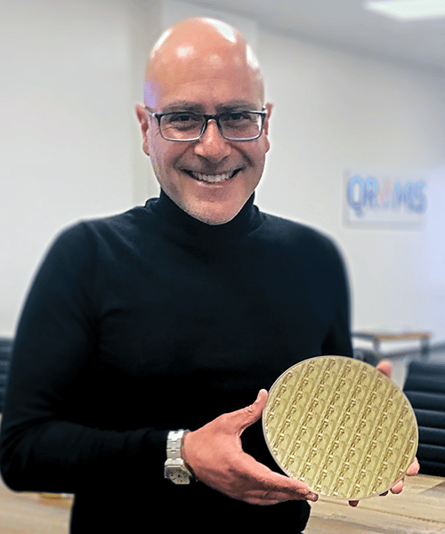
Cem Basceri, QROMIS president and CEO, displays a 200-mm-diameter 650 V, E-mode gallium nitride discrete power device wafer on a QROMIS Substrate Technology (QST®) substrate.
ADVERTISEMENT

Q. What are the current applications of GaN?
A. GaN is most commonly encountered in the commercial marketplace through LED lighting. GaN-based LED lighting fixtures exhibit energy efficiency improvements of more than 85% compared to similar incandescent fixtures.
GaN is also used in power conversion applications, such as mobile chargers, consumer power supplies, data centers, solar inverters, and electric vehicle power. In these applications, GaN-based devices can help to reduce power losses by up to 10x. GaN is used in wireless communication applications as well, such as 5G and beyond. In these applications, GaN-based devices can help to improve the efficiency and range of wireless signals. This improvement is due to the ability of GaN-based devices to switch currents at much higher frequencies than silicon-based devices.
Finally, GaN is used in display technologies, such as microLEDs. MicroLEDs are a new type of display that is being developed to replace LCDs and OLEDs. GaN-based microLEDs can be used to create high-resolution displays with low power consumption.
Q. Do you expect GaN to replace silicon, or will the future be a portfolio of semiconductor materials for engineers and designers to select from?
A. Compared to conventional silicon-based devices, GaN-based power devices have demonstrated higher switching frequencies and power densities, as well as greater power conversion efficiency with simplified topologies. Because of these benefits, consumer applications for GaN, such as power adapters, have already seen widespread adoption and are growing exponentially. Industrial applications, such as electric vehicles and power supplies for data centers and solar inverters, are expected to follow by 2030.
It is expected that both GaN- and silicon carbide (SiC)-based power devices will co-exist with silicon-based devices for a while; however, a complete switch over to these alternative semiconductor materials is expected in a few decades.
Q. What challenges must be overcome to further expand the use of GaN in commercial applications? How is QROMIS approaching these challenges, and what progress has been made?
A. There are no fundamental material barriers to scale-up and mass production of GaN. Instead, the main barrier to widespread GaN adoption is the lack of both a scalable and low-cost substrate technology for GaN electronics.
To date, commercial products containing GaN have relied on substrates with low performance and high mismatch in the thermal expansion (e.g., silicon, sapphire, silicon-on-insulator). To achieve widespread GaN adoption, it will require the development of a substrate with a more closely matched thermal expansion that is scalable, high-yielding, wafer breakage-free, CMOS compatible, and SEMI standard thickness. Such a substrate will enable economies of scale and a full spectrum of low-cost, reliable products, such as lateral and vertical power switches extending from 100 V to 1,800 V and beyond, in discreet and monolithic integrated circuit (IC) forms.
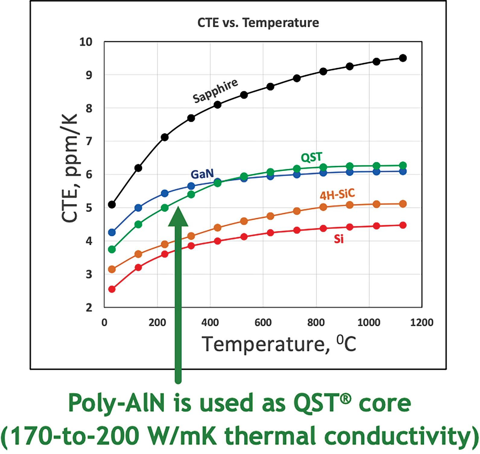
QROMIS’ disruptive commercial solution—which enables high volume, wafer breakage-free, low cost, and scalable GaN power device manufacturing—is the CMOS fab-friendly and SEMI standard thickness engineered substrate called QST®. This substrate has a core based on polycrystalline aluminum nitride (AlN) with a thermal expansion that very closely matches the thermal expansion of the GaN/AlGaN epitaxial layers. This groundbreaking solution allows for GaN epi thickness scaling as well as enables a confident roadmap to 300-mm-diameter GaN production.
Coefficient of thermal expansion (CTE) versus temperature for GaN and different substrates.
Credit: QROMIS
Proprietary engineered layers wrapped around the AlN ceramic core, followed by a buried oxide and thin top silicon (111) nucleation surface, result in a wafer that meets CMOS fab compatibility at standard SEMI specifications and with less than 3-mm edge exclusion.
The AlN ceramic core of the QST is also electrically insulating and compatible with the manufacture of radio frequency devices due to low absorption loss, unlike silicon. It has a thermal conductivity of 170–220 W/mK, which is higher than that of silicon.
These unique features enable not only mainstream lateral GaN power devices but also the long-awaited commercial and low-cost vertical GaN power switches and rectifiers suitable for high voltage aand high current applications presently dominated by limited-performance silicon insulated-gate bipolar transistors and high-cost SiC power field-effect transistors and diodes.
Currently, both QROMIS and its licensee Shin-Etsu Chemical Co., Ltd. (SEC) offer commercial 150-mm and 200-mm QST substrates and GaN-on-QST epitaxy wafers for worldwide GaN device manufacturers. 300-mm-diameter commercial products are targeted to be offered in the 2024–2025 timeframe.
Q. In November 2022, Vanguard International Semiconductor (VIS) in Taiwan started mass production of the first 200-mm, 650 V GaN power chip using the QST substrate technology under license from QROMIS. How significant was this breakthrough? What would be the next scale-up milestone?
A. VIS’ 200-mm GaN-on-QST processing technology is remarkable for two reasons. One, it is the first time that a company has offered 200-mm GaN device foundry services on a scalable and CMOS fab friendly QST platform for all GaN industry players. Two, this breakthrough was achieved in only five years, from ground-zero in 2018 to the release of products in 2023. Most other GaN device manufacturers spent 10+ years to achieve commercialization with very limited performance on non-QST substrates.
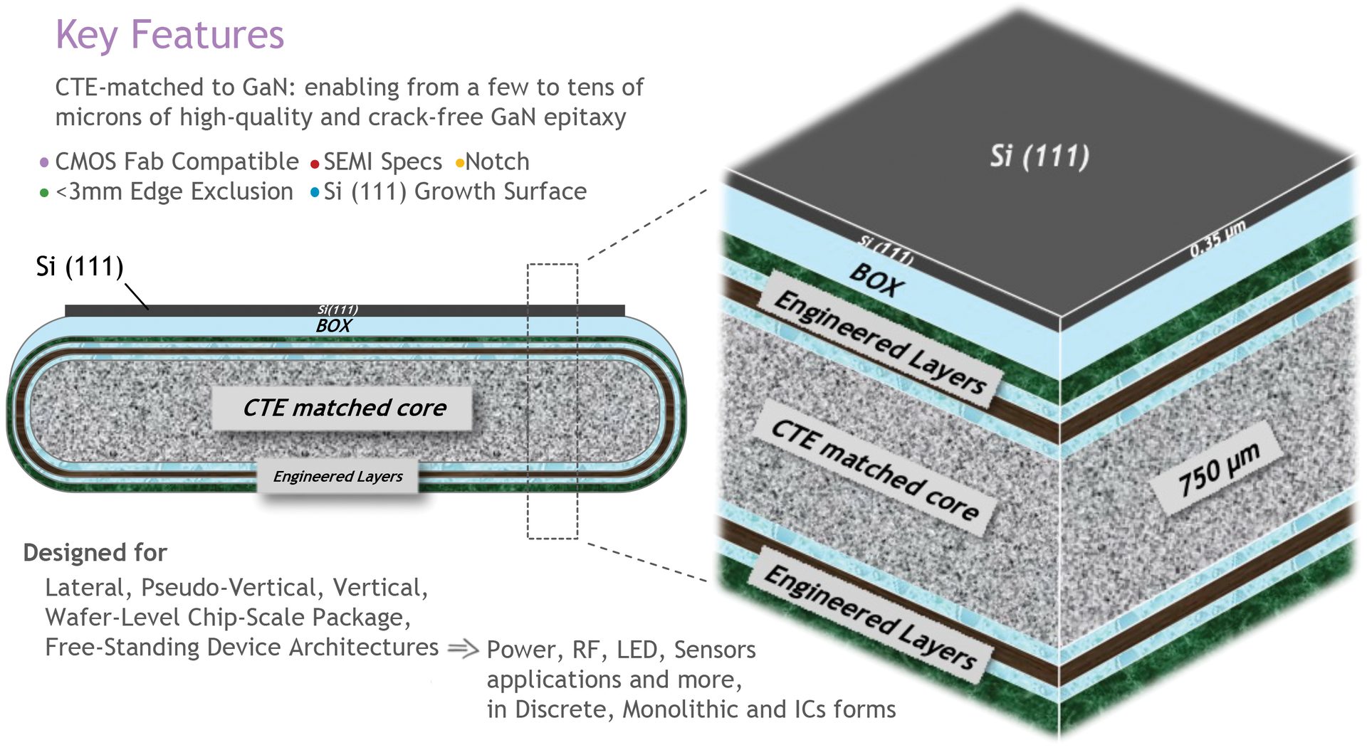
The CMOS fab-friendly, SEMI Spec QST substrate structure.
Credit: QROMIS
In 2018, VIS adopted QROMIS’ QST technology for a processing development of 0.35-µm 650 V GaN-on-QST on 200-mm substrates. The processing technology was completed in Q1 2022, and it successfully entered the mass production phase in Q4 2022. VIS simultaneously launched several collaborations with domestic and overseas integrated design manufacturing vendors and IC design companies.
VIS’ 0.35-µm 650 V GaN-on-QST processing technology is compatible with the development and production of the company’s existing 200-mm silicon wafer equipment, thus allowing it to achieve optimal production efficiency and product yield performance. Moreover, with the superior thermal property of QST substrates, GaN wafers produced by VIS achieve better overall heat dissipation performance for fast-charging solutions. In fact, based on the results of system verification at the customer end, products using the GaN wafers provided by VIS that address the fast-charging market for greater than 65 W have achieved world-leading performance.
In addition to the option of 650 V components, VIS’ GaN-on-QST processing technology also offers customers with add-on and robust electrostatic discharge as a flexible design option. Not only does VIS GaN technology platform offer greater device reliability, but VIS also launched cooperation with multiple customers for development of scalable device technologies for higher voltage applications (greater than 1 kV) to satisfy their product needs.
SIDEBAR
Gallium nitride technology innovator
QROMIS, founded by Cem Basceri and Vladimir Odnoblyudov in 2015, is a privately held fabless technology innovator headquartered in Santa Clara, Calif. The company, with its global partners Micron Technology Inc., Vanguard International Semiconductor Corp. (VIS), Shin-Etsu Chemical Co., Ltd. (SEC), SPARX Group Co., Ltd, and Tokyo Electron Ltd. Venture Capital, is a premier player in the rapidly growing, multibillion dollar energy efficient GaN electronics industry. Its disruptive and patented engineered substrate technology innovation (more than 200 worldwide patents) enables an unmatched cost, performance, and application scale for GaN power electronics.
As a rapidly growing Silicon Valley-based fabless company, QROMIS is driving the commercialization of its groundbreaking and patented engineered substrate innovation by leveraging the manufacturing platforms of its worldwide industrial partners and customers through close collaborations, up and down the supply chain. Commercial QST® substrates are available from QROMIS and SEC in 150-mm and 200-mm diameters (300-mm diameter coming in 2024–2025) for 100 V to 1,800 V and beyond high-performance GaN discreet and wafer-level monolithic IC power devices. In parallel, VIS, as a pure-play foundry, offers 200-mm GaN-on-QST power device foundry services for all industry players.
GaN-based devices built on the new and disruptive QST substrate technology will dramatically reduce global energy use and consumption. Markets served include power electronics, light emitting diodes, advanced displays, and RF electronics, and other emerging high-performance and energy-efficient applications.

Additional reading
- J. Raynel Koch, “GaN wide bandgap semiconductor enabling 1200 V and beyond power switches, now commercially available for 200-mm large-scale manufacturing,” U.S. Naval Research Laborator. Published 7 June 2021. Accessed 24 July 2023.
- “VIS 0.35 µm 650 V GaN process enters mass production,” VIS. Published 22 Nov. 2022. Accessed 24 July 2023.