
When smaller is better: The promise of nanomaterials
By David Holthaus
In a world where bigger often equates to better, nanotechnology flips that on its head: smaller is superior. The relatively young science makes use of rapidly evolving research to exploit the unique properties that materials display when they are in the nanoworld, far too small to be seen by the naked eye.
A nanometer is one-billionth of a meter. Imagining something that small can be difficult, so it helps to describe this measurement in everyday terms. A sheet of paper is 100,000 nanometers thick. A human hair is about 80,000 nanometers wide. One inch equals 25.4 million nanometers.
Nanomaterials can come in different sizes and shapes, as long as at least one dimension is on the nanoscale (< 100 nm). For example, nanoparticles and quantum dots have all their dimensions on the nanoscale, while nanorods and nanofibers are confined to the nanoscale in two dimensions but can be longer in the third.
Some trace the advent of nanotechnology to a groundbreaking lecture in 1959 by Nobel Prize-winning physicist Richard Feynman at the California Institute of Technology.
“Atoms on a small scale behave like nothing on a large scale, for they satisfy the laws of quantum mechanics,” he said during the lecture. “So, as we go down and fiddle around with the atoms down there, we are working with different laws, and we can expect to do different things. We can manufacture in different ways.”
At the atomic level, Feynman said, scientists will see “new kinds of forces, new kinds of possibilities, and new kinds of effects.” But, he noted, “The problems of manufacture and reproduction of materials will be quite different.”
ADVERTISEMENT

From research to application
Although Feynman’s lecture was delivered nearly 65 years ago, it was in the 21st century that the promise of nanotechnology began to materialize in many industrial sectors, including medicine, energy, information technology, and environmental science. That is when researchers and manufacturers gained the tools and techniques necessary to image and manipulate materials on the nanoscale.
Nanomaterials allow for products to be made lighter, stronger, more durable, more reactive, and/or more conductive, among other properties. For example, nanoscale additives in personal body armor can make it lighter yet more protective. Nanoscale films on glass can make eyeglasses, computer screens, and cameras more water-repellent, anti-reflective, and self-cleaning. Nanoengineered materials in cars are found in high-power, rechargeable battery systems; thermoelectric materials for temperature control; and tires that improve fuel mileage. Nanostructured ceramic coatings improve wear resistance for machine parts, while nanoscale lubricants and engine oils can extend the lifetimes of moving parts in everything from power tools to industrial machinery.
In the United States, the National Nanotechnology Initiative (NNI) was launched in 2000, bringing together more than 30 federal departments, independent agencies, and commissions to work together on understanding and controlling matter on the nanoscale. Its main areas of focus include leveraging nanotechnology to improve water sustainability, sensors, and electronics.
The NNI coordinates investments in nanoscale research and development across the U.S. government. Cumulatively, the participating government agencies and departments have invested more than $38 billion over the past 20 years to realize the potential of nanoscience, the agency says.
One company that produces nanomaterials is Cerion, a Rochester, N.Y.-based firm that designs, scales, and manufactures metal, metal oxide, and other ceramic nanomaterials for companies that are developing products and systems that will use them.

ADVERTISEMENT

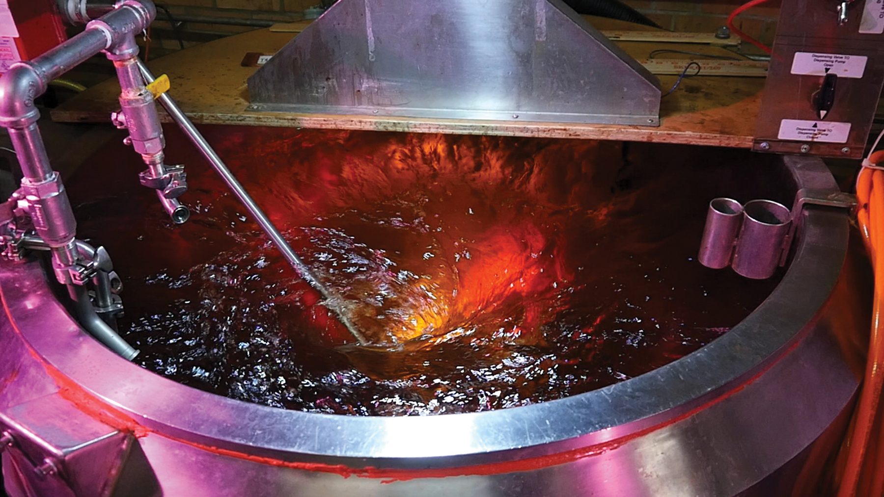
A large-scale reactor mixes nanomaterial product at Cerion’s manufacturing plant. Credit: Cerion

A nanomaterial sample from a large-scale reactor in Cerion’s industrial-scale manufacturing facility. Credit: Cerion
“We’re one of the oldest and one of the largest in the United States for manufacturing nanomaterials,” says CEO Landon Mertz. “We’re about 16 years old now, which, at least in our industry, makes us a dinosaur. It’s still a very young industry.”
Although Cerion was founded in 2007, its history goes back much farther to Rochester-based photography pioneer Eastman Kodak Company, which developed the precipitation-based manufacturing processes for fabricating materials used in photographic film emulsions. Building on that work, Cerion researchers developed processes to create and scale up nanomaterials to satisfy customer specifications.
Some of the main challenges in the nanomaterials industry include being able to rapidly design custom materials specific to a product or system while preserving the material’s technical attributes during scale-up and manufacturing. Plus, they must accomplish these goals in a cost-efficient manner.
Some manufacturers may customize off-the-shelf materials or invest in bringing nanomaterial expertise in-house, but this approach can be costly. Cerion focuses on designing and scaling nanomaterials to meet specific customer needs.
“We provide product development teams and commercialization teams with access to advanced expertise in precision design, scale-up, and manufacturing so that our customers can get access to nanomaterials at commercial scale,” Mertz says.
In its earlier years, Cerion scientists saw demand for nanomaterials that can modify the refractive index in glass for use in mobile phone displays, television displays, and augmented reality. But over the last few years, Mertz says the demand in the ceramics market has shifted toward powders.
“What you tend to see is somebody’s making a part that is either wholly or partially comprised of a nanomaterial that then gets incorporated into a larger system,” he says.
Nanomaterials are a general-purpose technology, Mertz says, a technology that can be implemented across the entire economy throughout a wide range of industries.
“We tend to see demand across almost every major industrial sector, but it tends to be on the higher-value end of the spectrum,” he says.
In the ceramics sector, the biomedical field is the most explored, as ceramic nanoparticles are considered good carriers for drugs, genes, proteins, and imaging agents, according to researchers at Jamia Hamdard University in New Delhi, India. They say nanoparticles have been successfully used as drug delivery systems against bacterial infections, glaucoma, and, most widely, cancer.

Landon Mertz
Next-generation electronics
The field of 2D materials is where some of the most leading-edge nanomaterials research is conducted today. 2D materials are a class of nanomaterials that are merely one or several atoms thick, but they have properties that include being exceptionally strong, lightweight, flexible, and excellent conductors of heat and electricity.
At The Pennsylvania State University’s Materials Research Institute, Joshua Robinson and his team are working on creating 2D materials for applications in next-generation electronics beyond silicon for digital circuits and flexible electronics, as well as developing novel coating technologies and functionalities enabled by 2D materials.
“The 2D materials we focus on are made on a flat surface and grown over very large areas,” Robinson says. “We can make these so that they’re compatible with the standard electronics industry. Our aim is to manufacture them in a way that is useful for folks like Intel that are working hard on next-generation transistors and things like that.”
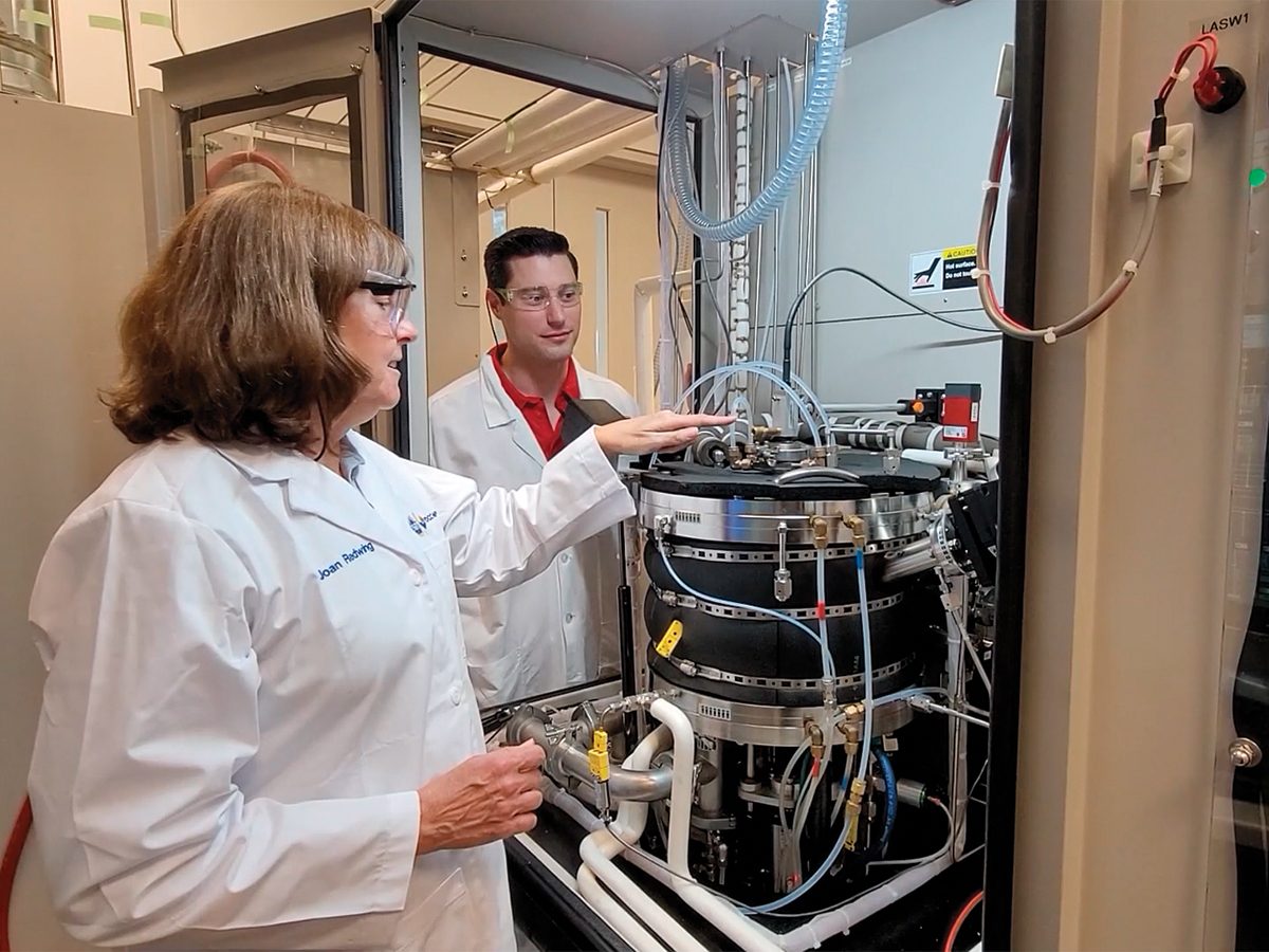
Joan Redwing, left, leads research at Penn State’s 2D Crystal Consortium-Materials Innovation Platform lab. Credit: Seana Wood, Penn State
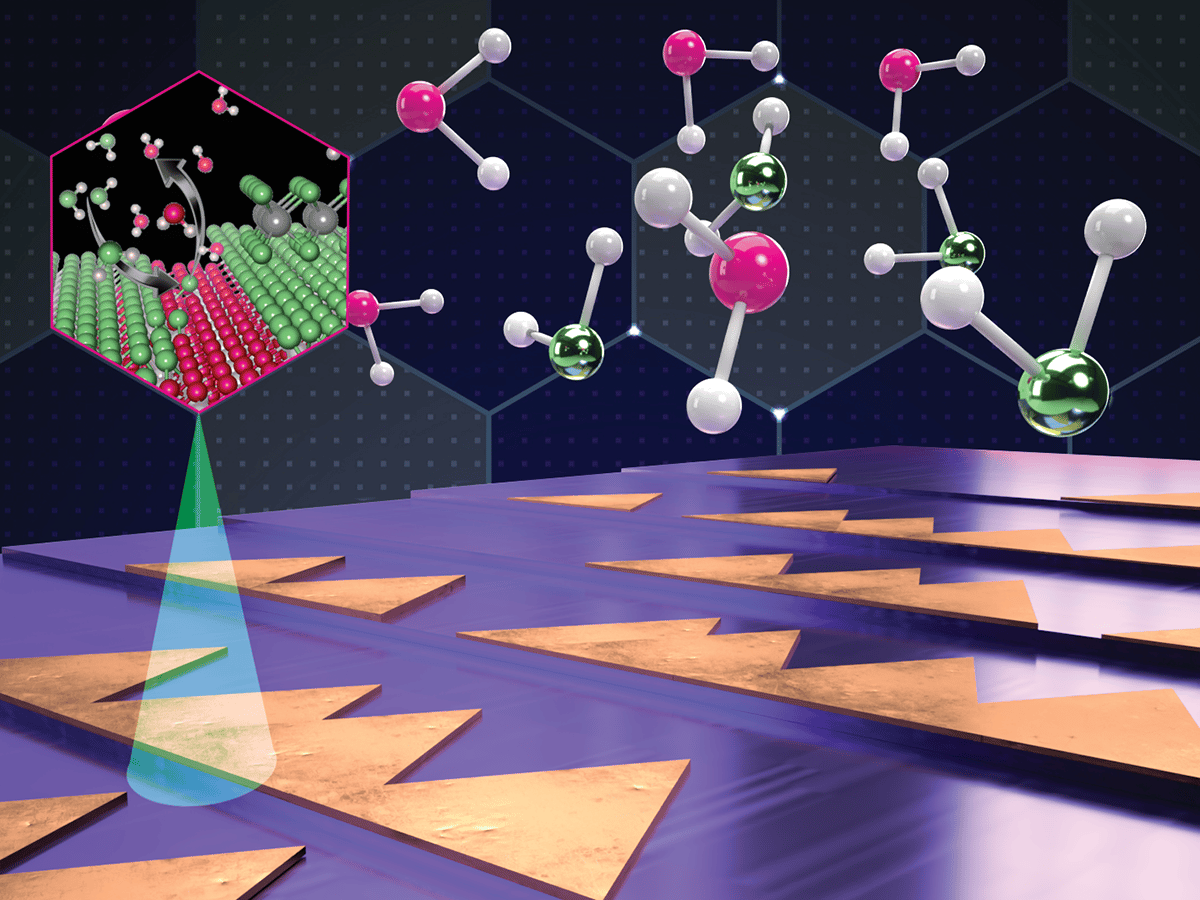
Atomic-scale steps on sapphire substrates enable crystal alignment of 2D materials, reducing defects and improving electronic device performance. Credit: Jennifer M. McCann, Penn State
Graphene, a 2D material consisting of carbon atoms arranged in a honeycomb-like structure, is made by researchers in Penn State’s 2D Crystal Consortium-Materials Innovation Platform lab using a small furnace that heats elements to 2,400°C. Graphene is very strong but also super thin, which allows electrons to move much faster through it than they can through silicon, the basis of today’s computer chips.
Replacing silicon with graphene may allow computers to transmit information much faster than they already do and make them even more energy efficient. But before they can be manufactured at industrial scale, they must be produced and perfected in places such as Robinson’s lab.
Although the focus of Robinson’s lab currently is semiconductors, there are many other applications for their research.
“There’s use of these materials in things like catalysis and hydrogen evolution for energy,” he says. “There’s also materials for photovoltaics, like solar cells.”
Europe’s investment in graphene
Graphene was first isolated in 2004 by two researchers at the University of Manchester, U.K. Since then, research on this ultrathin and ultrastrong material has exploded, and it can be found in commercial products including lithium-ion batteries, motorcycle helmets, and lubricants in high-power electronics.
Several groups in Europe are leading the charge on graphene research. For example, the University of Manchester now houses the National Graphene Institute and the Graphene Engineering Innovation Centre. A team of scientists there in January 2024 announced they had received a 3-million-euro investment to help them develop a lithium-free energy storage solution.
Additionally, in 2013, the European Union formed a consortium of industry and academic partners called The Graphene Flagship. The initiative was one of three established by the European Commission to investigate major, long-term scientific and technological challenges. The others are a project on the human brain and one on quantum technologies.
The effort was initially funded with one billion euros from the European Commission and focused largely on academic research. It gradually evolved to industry-led projects using the research gained from its initial work, says Patrik Johannson, director of the Graphene Flagship.
“Our overall vision over these years has been ‘from lab to fab[rication],’” he says.
Research conducted through the Flagship has led to 83 patents, and 17 spin-off companies have been generated from it, according to the consortium’s latest annual report. So far, the Flagship has convened 11 industry-led projects that are focused on real-world applications.
The Flagship’s industry partners include Fiat-Chrysler (Amsterdam, Netherlands), which is working on a dashboard for vehicles that will feature conductive patterns, sensors, and other devices based on graphene. Sweden-based energy giant ABB is working on a maintenance-free circuit breaker that would replace grease in drive mechanisms with self-lubricating graphene. And aerospace company Lufthansa is working on a project to improve air filtration systems in aircraft using graphene foams.
The versatility of graphene and its potential to be used in such a broad range of applications led to the European Union’s effort, Johannson says. But he notes the cost of the material varies depending on its application.
“Do you want it to be for wafer production? Or do you want it as a filler in concrete? You can imagine that’s quite different,” he says.
The costs of nanomaterials may adjust as their applications become more accepted in the marketplace, says Cerion’s Mertz.
“The way we need to look at it is how do we get more volume into the marketplace, which helps bring some fixed costs down,” he says. “The people that tend to adopt new technologies need some kind of new leading-edge performance. And they are willing to pay for it. You’re first to market. Over time, as you ramp up volumes, you’re able to make these materials more mass-market.”
Significant challenges remain in converting research lab findings to industrial applications and in scaling up production, which includes controlling for cost. Other challenges, particularly with biomedical materials, include gathering long-term information on their safety. And standards for the industry are still under development, making it difficult to develop regulatory guidelines.
But thanks to more than two decades of basic research, investment, and application, it is almost certain that these challenges will be overcome, allowing nanotechnology to improve and even revolutionize many more technology and industry sectors.
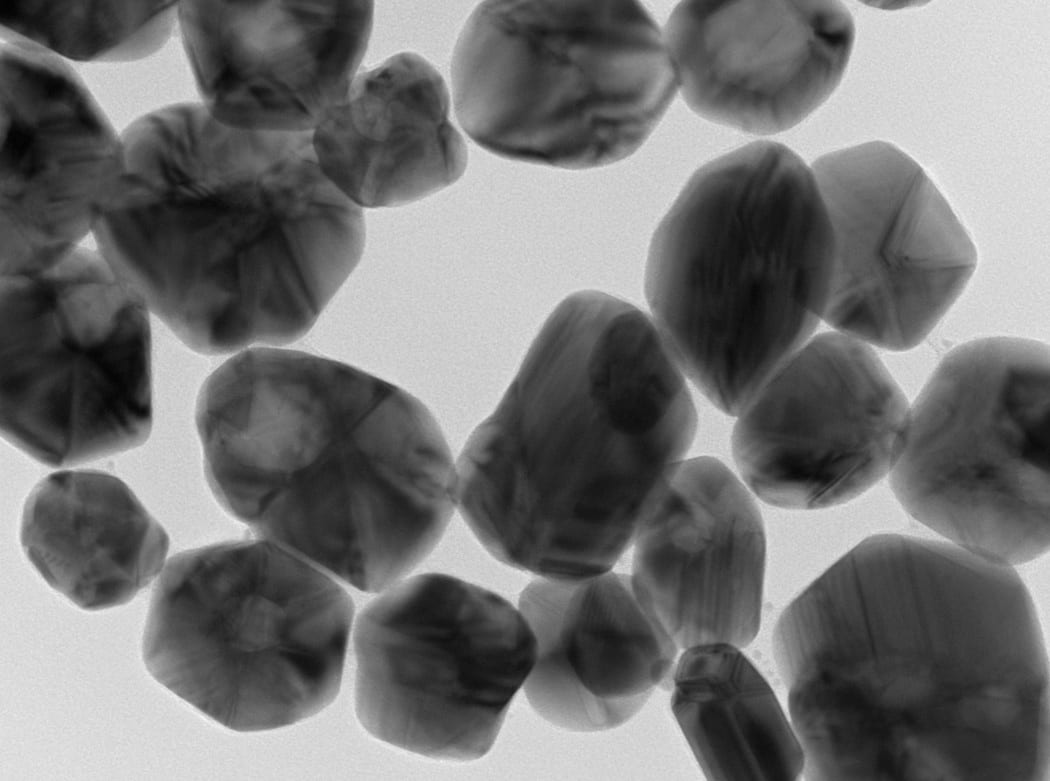
An electron microscopy image of silver nanoparticles. Credit: Cerion
An electron microscopy image of silver nanoparticles. Credit: Cerion
SIDEBAR
Nobel Prize winners in nanoscience
By David Holthaus
Over the last decade-plus, the Royal Swedish Academy of Sciences has awarded several Nobel Prizes for groundbreaking research in nanomaterials.
In 2023, the Nobel Prize in Chemistry was awarded to a trio of scientists for the discovery and development of quantum dots, nanoparticles so tiny that their size determines their properties. Quantum dots now illuminate computer monitors and television screens based on QLED technology. They also add depth to the light of some LED lamps, and biochemists and doctors use them to map biological tissue.
Physicists had long known that, in theory, size-dependent quantum effects could arise in nanoparticles, but it was considered almost impossible to design materials on that scale with precision. So, few believed this knowledge could be put to practical use. But in the early 1980s, Aleksey Yekimov, now the chief scientist at U.S. company Nanocrystals Technology (New York, N.Y.), succeeded in creating size-dependent quantum effects in colored glass. The color came from nanoparticles of copper chloride. Yekimov demonstrated that the particle size affected the color of the glass via quantum effects.
A few years later, Louis Brus of Columbia University was the first scientist to demonstrate size-dependent quantum effects in particles floating freely in a fluid. Then in 1993, Moungi Bawendi of Massachusetts Institute of Technology revolutionized the chemical production of quantum dots, resulting in a high quality that was necessary for them to be used in applications.
“They planted an important seed for nanotechnology,” the Royal Swedish Academy said in awarding the coveted prize.
In 2010, the Nobel Prize in physics was awarded to two scientists at the University of Manchester in the United Kingdom who first unambiguously produced and identified the 2D material graphene. Andre Geim and Konstantin Novoselov extracted a single-atom layer of carbon from a piece of graphite using ordinary adhesive tape. Their groundbreaking work was done at a time when many believed it was impossible for such thin crystalline materials to be stable.
Today, graphene is known to be a conductor of electricity that performs as well as copper. As a conductor of heat, it outperforms all other known materials. It is almost completely transparent, yet so dense that not even helium, the smallest gas atom, can pass through it. Because of these properties, it has applications in batteries, transistors, and computer chips, among others.