Engineering SiC quantum systems through precision implantation and analysis
By Nazar Delegan
bulletin | feature
Silicon carbide holds much promise as a platform for quantum systems. New research at Argonne and Sandia National Laboratories unlocks this potential through precision engineering and analysis.
Quantum information science holds immense promise for revolutionizing computation, communication, and sensing. Central to these advancements are solid-state defect centers in wide bandgap semiconductors.
Defect centers are tiny imperfections in a material’s atomic lattice caused by various factors, including missing atoms (vacancies), atoms in places that are typically vacant (interstitial atoms), and the presence of foreign atoms not inherent to the material’s compositional makeup. These defects can have specific spin states associated with them. These discrete spin energy states can be used as quantum bits (qubits) for storing and manipulating information. While similar to the binary system of 0s and 1s in classical computing, qubits have added unique behaviors such as superposition, enabling significantly higher information density.
Diamond-hosted nitrogen-vacancy centers have attracted the most attention in the field of solid-state quantum information processing as possible spin defects for qubits. But silicon carbide (SiC), a sought-after wide bandgap semiconductor that is typically used for high-power electronic and harsh environment applications, also holds much promise as a quantum platform.1
SiC benefits from better material availability, scalability, and fabrication methodologies than diamond.2–4 Most importantly, SiC can host a variety of interesting optically active spin defects, some of which can be coherently driven at room temperature.
There are challenges with using SiC as a platform for quantum information systems, however, that must be addressed to enable scaling of this technology. Researchers at Argonne National Laboratory and Sandia National Laboratories recently conducted a study to address one of these challenges: implanting qubits in SiC with extreme precision.5 The results of their efforts are described in the sections below.
Challenges to scalable quantum technologies based on spin defects in semiconductors
Some of the most interesting optically active spin defects in SiC are the neutrally charged divacancy complexes (VV0), which consist of a neighboring silicon atom and carbon vacancy. These defects feature mid-gap electronic energy states, which separate them from the host material’s energy bands. This separation allows the defects to behave like isolated and discrete energy levels reminiscent of atomic systems, which, with the help of some intermediate energy levels, make it easy to initialize and readout the qubits’ spin states.2–4
While this “isolated atomic system” approximation is quite useful for quantum processing, designing and harnessing VV0 defects for use as qubits is extremely difficult. The energy level structures in these defects are defined by the intricate interplay between the defect’s symmetry group, spin-lattice coupling, and the broader host material’s electrostatic environment. This reliance on numerous variables makes the VV0 defects intrinsically sensitive to their local charge, magnetic, crystallographic, and strain environments—all of which can have diverse and difficult-to-quantify effects on the spin defect’s quantum performance.6
The inherent variability in spin-defect environments and, by extension, properties and performances poses a significant challenge to the deterministic and homogeneous synthesis of spin defects, limiting the full potential of defect-based quantum technologies. Because of this limitation, many state-of-the-art quantum demonstrations rely on pre-screened defects that are hand picked because they show the best properties for the intended experimental demonstration. Concurrently, any unidentified sources of variance are actively dismissed as being due to limited characterization capabilities at the relevant scales.
In response to this challenge, researchers globally are involved in a focused, multifaceted, and multimodal effort to understand the causes behind defect-to-defect variability on both the nano- and microscale. Understanding these causes will improve researchers’ deterministic and homogeneous synthesis capabilities.
The development of tools capable of generating and studying crystallographic defects has been essential to progress in this field of research. In the recent work led by Argonne and Sandia National Laboratories,5 we explored the interplay between VV0 spin defects and their host material (4H-SiC single crystal wafers ranging from a few mm to 6 inches) using a focused ion beam nanoimplantation technique developed at Sandia (see sidebar “Basics of nanoimplantation”) and X-ray nanodiffraction performed at the Advanced Photon Source at Argonne.7,8
i

ADVERTISEMENT
SIDEBAR
Basics of nanoimplantation
Nanoimplantation is a technique commonly used in the semiconductor industry. It enables the manipulation of material properties and behaviors by introducing a wide array of defects and dopants into materials at the nanoscale.
The approach involves extracting atomic species from a source material via thermal or electrostatic means, and then these ions are accelerated toward a solid target material. During impact, the energized ions will displace atoms in the target material and create defects, such as vacancies and interstitials, or embed themselves in the target material as dopants. The size, distribution, and type of defects generated can be tailored by precisely controlling the ion beam parameters, such as energy and dosage.
The nanoimplantation technique developed at Sandia uses a series of electromagnetic lenses to focus the accelerated ions down to areas as small as 25 x 25 nm2. Learn more about the specifics of the Sandia technique in References 7 and 8.
Mapping strain effects on the behavior of VV0 spin defects
The photoluminescence mapping in Figure 1a shows the precise control of VV0 synthesis in 4H-SiC that is possible using the ion beam nanoimplantation technique developed at Sandia. The implantation arrays were composed of identical implantation columns and fluence rows starting at 10,000 ions/spot and decreasing down to 10 ions/spot. The columns allowed for statistical repeatability, whereas the rows allowed for isolation of the implantation fluence effect and creation of a single defect regime.
The device used for nanoimplantation can allow for implantation spot sizes as small as 25 x 25 nm2. However, the equipment calibration was slightly off during testing (noticed post-situ), so the obtained implantation spot sizes were about 66 x 56 nm2.
Processing of the samples at 850°C in argon resulted in a significant increase of VV0 photoluminescence. This increase is explained by the diffusive mobilization of implantation-generated silicon and carbon vacancies, which formed additional divacancy centers while reducing local damage. Unfortunately, lower ion fluences did not reveal single VV0 defects with expected count rates, which may have been due to charge state instability from excessive local damage caused by implantation or insufficient thermal processing.
To better understand the mechanisms underlying these observations, we probed the local strain profiles at the defect scale using a nondestructive coherent nanoscale focused X-ray technique.9 The synchrotron X-ray beam was focused down to an effective pencil beam width of about 25 nm and rastered across an area of 0.5 µm by 1.3 µm with steps of 25 nm. The data obtained from this probe provided a full set of 2D detector diffraction data per spatial pixel of the sample projected along the direction of the exit beam. This data was then collapsed, normalized, and systematically fitted per-pixel with a two-component model.
The Gaussian component of the model represented the diffracting areas of the nanoimplantation spot (Figure 1b), while the Darwin component represented the pristine 4H-SiC bulk (Figure 1c). This mapping allows us to extract a lower bound 2D strain profile of each implantation spot, with in-depth information partly projected along the x-axis.
From this map of the data, a phenomenological model emerges. It shows a tensile nano-implanted core surrounded by a compressive bulk area with local strains of about 2 × 10⁻⁴ and 1 × 10⁻⁵, respectively, as shown in Figures 1b and 1c. The drastically increased strain in the as-implanted samples is in alignment with the difference in photoluminescence observed between these samples, requiring orders of magnitude lower excitation to achieve similar levels of emission as seen in Figure 1a.
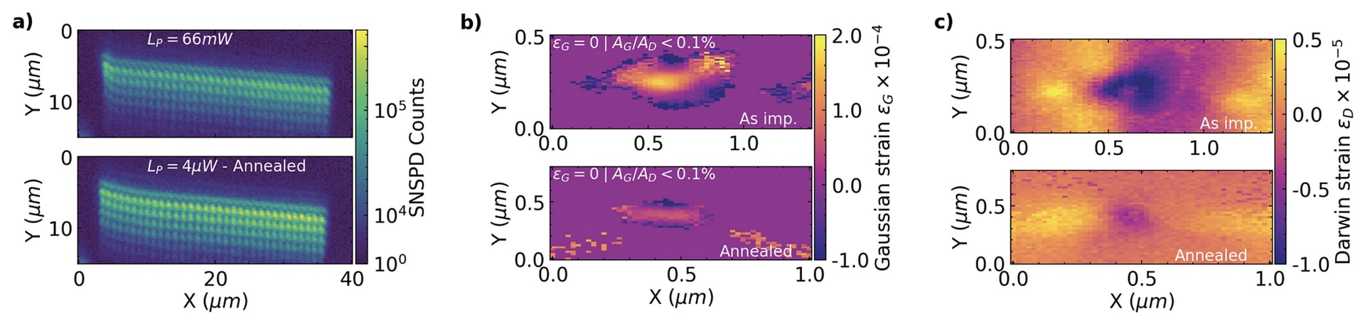
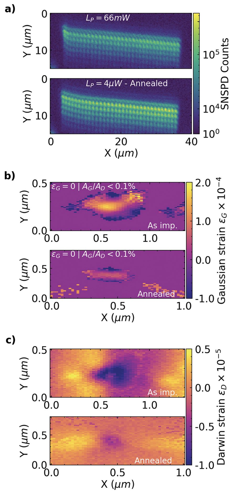
Figure 1. a) Photoluminescence map of VV0 defects obtained via silicon implantation of 4H-SiC with 10,000, 5,000, 1,000, 500, 100, 50, and 20 ions/spot per row, organized from top to bottom. The implantation array curvature is due to experimental error, resulting in initial array drift during implantation. LP is the laser power used to obtain the spectra.
b) 2D tensile strain profile extracted from the Gaussian component of the two-component fitting model for a 104 ion/spot implantation with the as-implanted spot shown above and the annealed spot below. The strain is set to 0 when the area of the Gaussian component is less than 0.1% of the Darwin component.
c) Strain response of the host 4H-SiC crystal extracted from the Darwin component for the as-implanted spot above and annealed sample below. It needs to be noted that the interaction volume from the Darwin and Gaussian components differ greatly and as such the extracted strain cannot be compared directly numerically, but it can be considered qualitatively.
Credit: Delegan et al., Nanotechnology (CC BY 4.0)
We note a drastic change in the overall local strain profile, indicating a diffusive-like strain relaxation mechanism with order of magnitude reduction in both the strain profiles post annealing. Work is ongoing to quantify these variations as a function of implantation fluences on the single defect level, as well as to develop more sophisticated thermal treatments.
Strikingly, our investigations revealed the presence of previously undocumented crystallographic features in 4H-SiC. For example, extended screw dislocations demonstrated large changes in the strain profile over short distances, specifically variations of 1.14 × 10⁻⁴ over 0.28 μm, as shown in Figure 2b.
This strain variation is likely underestimated due to the depth convolution of the strained features. But even at this lower bound for the observed strain, if two VV0 defects were to be located 0.28 μm away from each other (see theoretically plausible locations for P1 and P2 in Figure 2b), they would present a spectral shift of about 2.4 meV and 1.14 MHz for the zero-phonon line and ground-state splitting, respectively, as a result of the different strain environments of each defect (Figure 2a).
It is not unreasonable to propose that the large variation of material properties in a given material result from these ubiquitous and sparse crystallographic defects, which are found on the order equal to or more than 103 cm–2 (for thicknesses of 500 μm) in typical high-quality 4H-SiC. If a streamlined process for identifying these defects is implemented, it presents the possibility of using such local crystallographic defects to engineer unique systems and devices, paving the way for a slew of advanced quantum relevant control schemes.
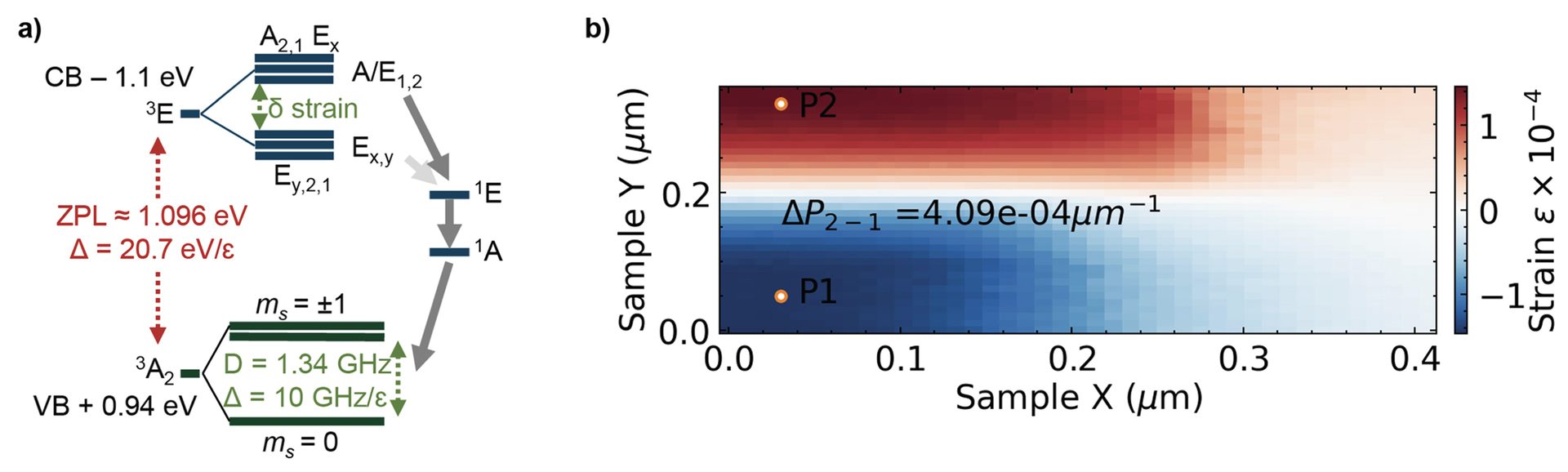
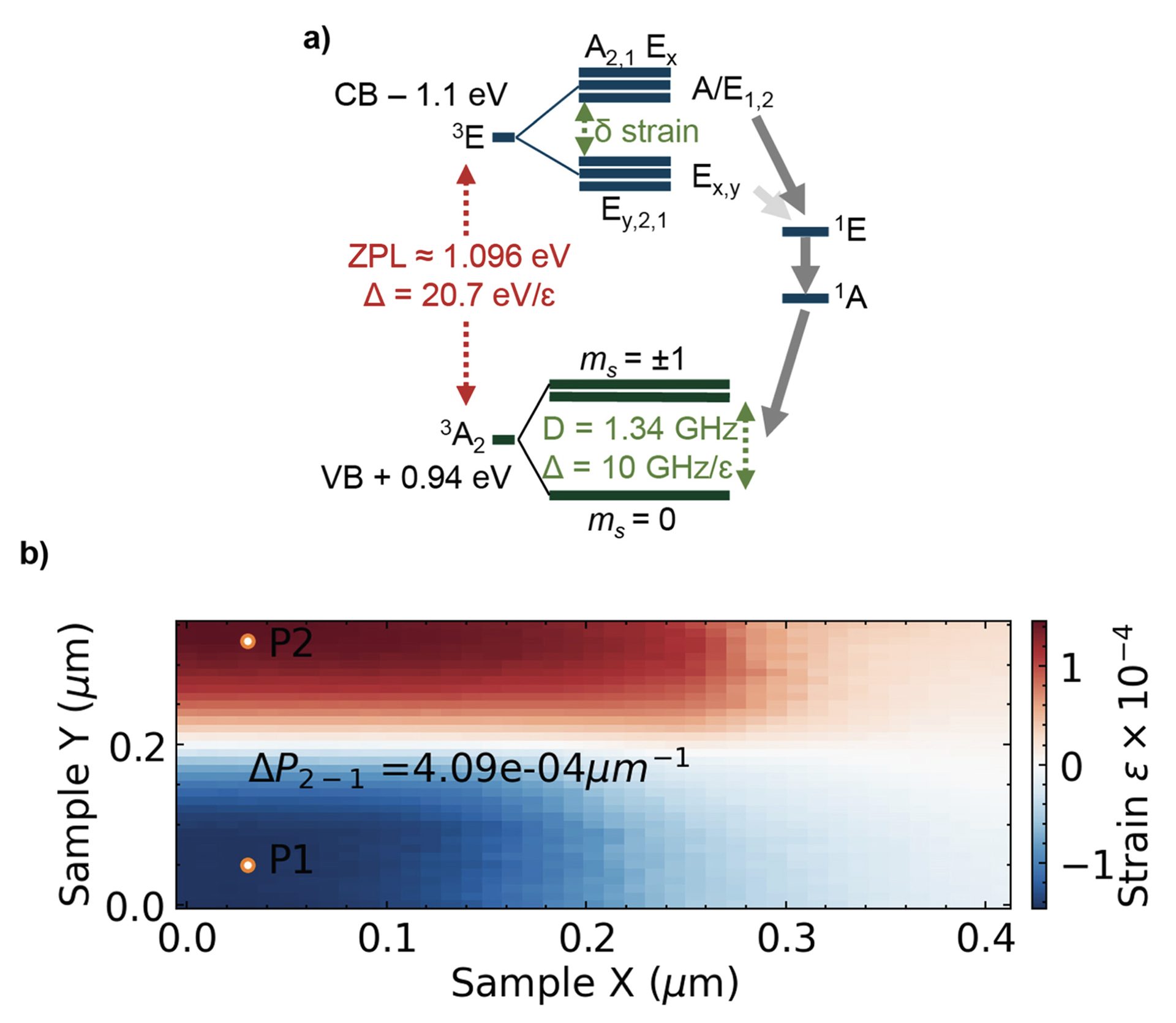
Figure 2. a) Energy level diagram of VV0 defects in 4H-SiC as a function of strain relative to the conduction band (CB) and valence band (VB).
b) At about 10 nm step size in a high-resolution raster nanodiffraction scan of a screw-dislocation running in-plane, we note a drastic change in strain from tensile to compressive, showing a 1.14 × 10⁻⁴ variation in strain over 0.28 µm. P1 and P2 are theoretically plausible locations for two VV0 defects within the same optical spot-size.
Credit: Credit: Delegan et al., Nanotechnology (CC BY 4.0)
Summary and outlook
Advancing the use of SiC as a platform for quantum information systems requires an understanding of the relationship between spin defects and their host materials at the nano- and microscales. This paper investigated the role of crystallographic attributes, namely strain profiles and lattice symmetries, in shaping the electrostatic environments and optical properties of quantum spin defects, focusing on the case of divacancy centers in 4H-SiC.
Our study reveals that local crystallographic features are the source of varied strain profiles and reduced lattice symmetries, leading to fluctuations in the optical properties of quantum spin defects. By conducting experiments at length scales of less than 1 µm, we gained insights into the inter-qubit variability in the solid state, laying the groundwork for strain engineering and deterministic localization of spin-defect systems.
Overall, the experimental platforms and demonstrations presented in this work contribute to the scalability and integration of quantum and classical technologies by understanding the inhomogeneity of spin defects and by demonstrating novel synthesis and characterization capabilities. By gaining a deeper understanding of defect formation dynamics and their manipulation at the nanoscale, we aim to harness the full potential of quantum spin defects for transformative applications in quantum computing, communication, and sensing.
About the author:
Nazar Delegan is assistant scientist in the Materials Science Division and Q-NEXT at Argonne National Laboratory (Lemont, Ill.). Contact Delegan.