Welcome to the ‘Emerging Professionals’ issue
bulletin | emerging professionals

By Michael Thuis
The modern student is entering an increasingly transient world. From artificial intelligence to quantum computing to climate change, the problems materials scientists and engineers face are growing more multifaceted. The next generation of ceramists must be prepared not only with a technical appreciation of their field but also a full social, ethical, and professional understanding to craft a successful career.
For students, fulfilling all these expectations is difficult to navigate alone. That is why, as an ACerS community, we are building a home for students to equip themselves with these essential skills and tools.
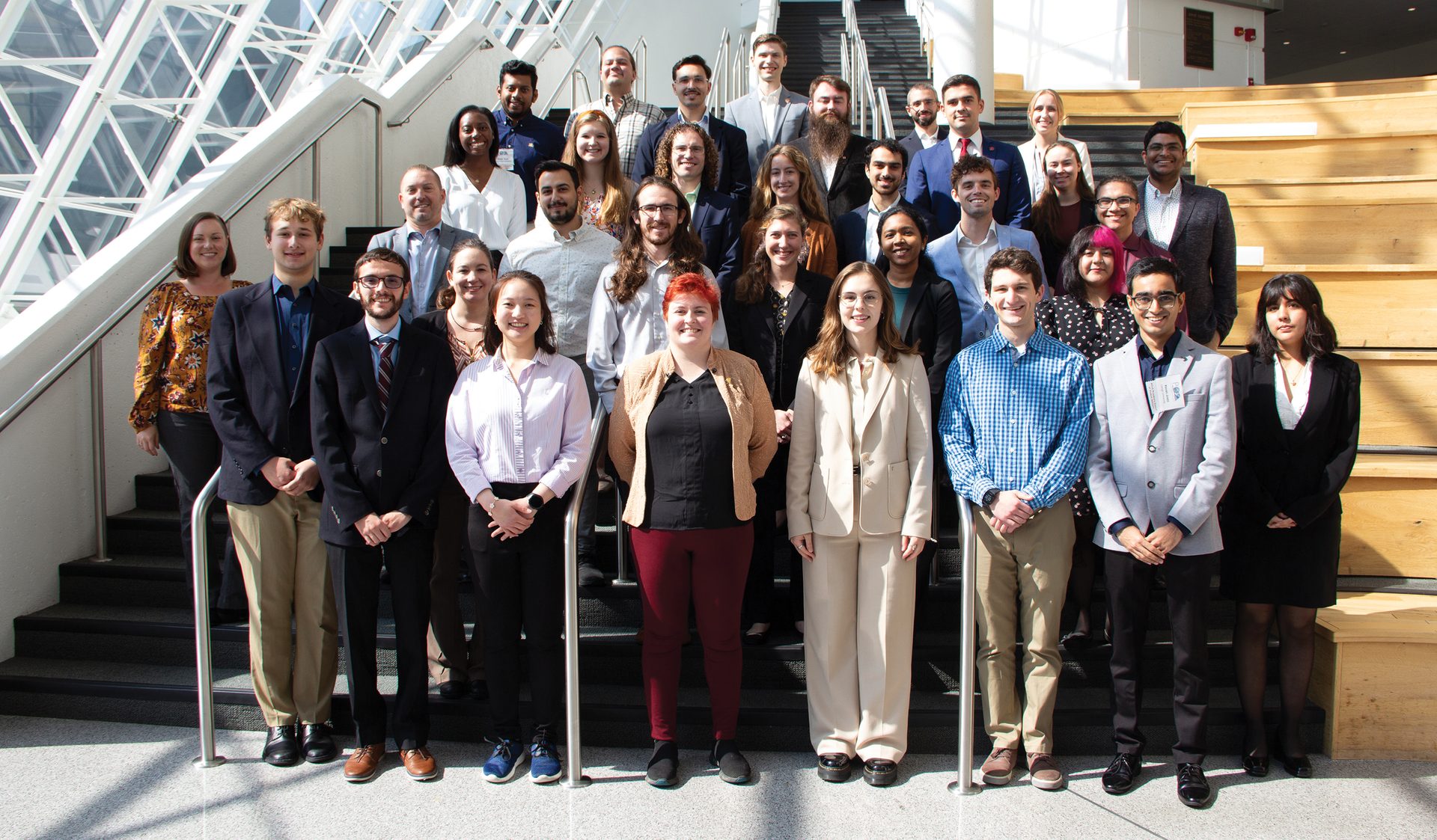
The ACerS President’s Council of Student Advisors is working this year to integrate these ideas further into the ACerS ecosystem. Halfway through 2024, the Council’s 38 delegates, from 19 universities and five countries, have already expanded new and existing programs through the PCSA’s five committees.
- The Conference Programming Committee arranged for student-focused activities at every ACerS conference in 2024. The Committee also created a conference guide to help students become oriented at their first conference.
- The Professional Development Committee continues to expand the library of ACerS student webinars focused on early career development. This expansion coincides with supporting IGNITE MSE, a new professional development program organized by the Ceramic and Glass Industry Foundation that runs in conjunction with select ACerS conferences.
- The Education Committee shared Materials Science Classroom Kit lessons and Mini Kits at the 2024 National Science Teaching Association conference, which is the largest conference for science teachers in the U.S.
- The Recruitment and Retention Committee worked tirelessly last year to recruit leaders from the ACerS community from nontraditional backgrounds, with a particular focus toward fostering the ACerS community in Africa. Their work allowed this year’s PCSA delegation to be the largest to date.
- The Communications Committee continues to grow the PCSA’s social media presence and is working to communicate PCSA initiatives with a broader scientific audience.
Michael Thuis
The 2023–2024 PCSA delegates at the PCSA annual meeting in October 2023.
Credit: ACerS
The PCSA Communications Committee also led the rebranding and expansion of the annual student section in this year’s June/July Bulletin. The new “Emerging Professionals” section aims to better showcase young ACerS members along every step of their journey, from undergraduates to recent graduates. The section consists of two parts:
- Research articles: Three full-page articles describe research based on this issue’s theme, “Ceramics for digital technologies.” These articles are contributed by Material Advantage, Global Graduate Research Network, and Young Professionals Network members.
- “Science for Society” articles: This two-page spread features three stories on the IGNITE MSE poster topics of outreach and community engagement; technology for social good; and inclusivity, diversity, and ethics in research.
This year also features two bonus articles contributed by ACerS members and staff, which describe the need for inclusivity in Q&A sessions at scientific conferences and the success of new diversity scholarships funded by ACerS, respectively.
I hope you find this year’s “Emerging Professionals” issue of the ACerS Bulletin insightful.
About the author
Michael Thuis is a Ph.D. candidate at Northwestern University studying in the Haile Lab. As the 2023–2024 PCSA Council Chair, he has worked to expand the presences of the PCSA in the ACerS community while sharing lessons learned.
Research articles
Material Advantage Student Program
The Material Advantage Student Program offers students membership benefits and access to The American Ceramic Society (ACerS), Association for Iron & Steel Technology (AIST), ASM International, and The Minerals, Metals and Materials Society (TMS). Learn more.
New architectures and materials for electronic packaging
By Javier Mena-Garcia
It can be difficult to imagine our daily routine without the electronic devices and gadgets that enable everything from our energy infrastructures to transportation systems to communication networks. The importance of electronics to modern life is recognized by the outpouring of funding and initiatives in recent years to support the manufacture of semiconductor chips,1 which form the heart of today’s electronics.
Developing new ways to package semiconductor chips is a focus of these programs. Traditionally, the performance of electronic devices was improved by making semiconductors smaller, which allowed more to be placed on each chip and increased processing power. However, semiconductors are now so small they are running up against the laws of physics. So, instead of shrinking chips further, designing novel strategies for combining (packaging) semiconductors together can reduce power consumption and increase processing power.2
3D packaging is an emerging approach to chip design that involves using traditional circuit connection methods to achieve vertical stacking of memory layers directly on a processor chip. This architecture provides the benefits of miniaturization while also reducing the time required for data transfer due to the processing and memory chips being closer together. To make the most use out of this architecture, however, ferroelectric materials that can be deposited at low temperatures on the chip must be developed.3
In addition to new architectures, designing materials with enhanced electrical and thermal properties is another way to improve the performance of electronics. For example, ceramic matrix composites (CMCs) may play a role in future circuits.
CMCs consist of fibers, modifiers, and filler materials placed within a ceramic matrix. CMCs are frequently talked about in the context of aerospace structural components, but they are also being considered for use in electronics because, depending on the fillers, they can exhibit higher thermal conductivity and higher electrical resistivity while simultaneously preserving a low dielectric loss.

READ MORE
As a Ph.D. candidate in professor Clive Randall’s group at The Pennsylvania State University, I have investigated the feasibility of fabricating CMCs for electronics using cold sintering.4 Cold sintering uses a transient transport phase (typically liquid) and pressure to enable densification of a ceramic system at much lower temperatures than traditional methods.5
To achieve CMCs with low dielectric loss and enhanced thermal conductivity, we engineered grain boundaries in the ceramic matrix using filler materials with strong covalent bonds and wide band gaps, such as hexagonal boron nitride and diamond (Figure 1). The integration of these fillers into the CMC also decreased the composite’s effective relative permittivity, brought the thermal coefficient of resonance frequency closer to zero, and improved the electrical insulation breakdown strength.
I feel fortunate to conduct research that advances the electronics field. The scientific discoveries and inventions we have and will make are key to realizing a more sustainable world.
References
1 The White House, “Fact sheet: CHIPS and Science Act will lower costs, create jobs, strengthen supply chains, and counter China.” Published 9 August 2022.
2 H. Tomoshige, “CHIPS+ and Semiconductor Packaging,” Published 7 November 2022.
3 W. Mills, “Over $10 million awarded to Penn State for energy center,” Published 25 July 2020.
4 Mena-Garcia Jet al. “Sodium molybdate-hexagonal boron nitride composites enabled by cold sintering for microwave dielectric substrates.” J Am Ceram Soc. 2023, 106: 5975–5985.
5 A. Ndayishimiye et al., “Reassessing cold sintering in the framework of pressure solution theory,” Journal of the European Ceramic Society 2023, 43(1): 1–13.
About the author
Javier Mena-Garcia is a Ph.D. candidate in materials science and engineering at The Pennsylvania State University. He studies structure–property relationships in ceramic matrix composites enabled by cold sintering. He is a Fulbright alumnus from Mexico, who enjoys going on long road trips with his wife, Cristy, and playing basketball.
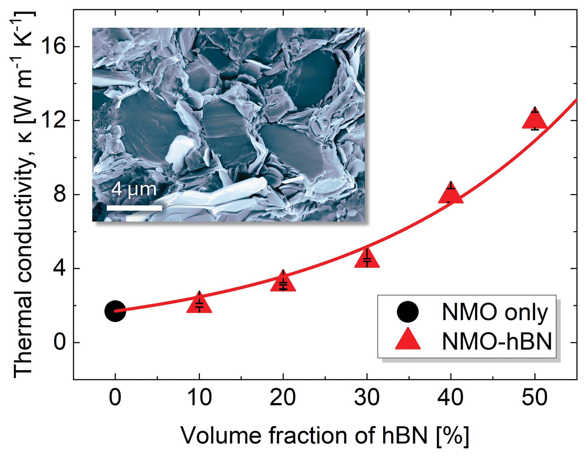
Figure 1. Inset picture: Scanning electron microscopy image of engineered microstructure of sodium molybdate (NMO) with 40 vol.% of hexagonal boron nitride (hBN) filler, enabled by cold sintering. Main graph: Improvement of thermal conductivity as a function of filler volume fraction. Adapted from Reference 5.
Credit: Mena-Garcia et al., Journal of the American Ceramic Society (CC BY-NC-ND 4.0)
COLLAPSE ARTICLE ABOVE
ACerS Global Graduate Research Network
ACerS Global Graduate Researcher Network (GGRN) membership addresses the professional and career development needs of graduate-level research students who have a primary interest in ceramics and glass. Learn more.

The ins and outs of multilayer ceramic capacitors
By Sevag Momjian
Long gone are the days when computers filled an entire room. Now, digital devices the size of your palm can perform operations in seconds that used to take computers days.
Miniaturization of these electronic packages results from smaller circuit components and compact hybrid integrated circuit designs. These circuits consist of active and passive components. Active components, such as transistors, perform all computational and memory processes. Passive components supply charge to the processing chips.
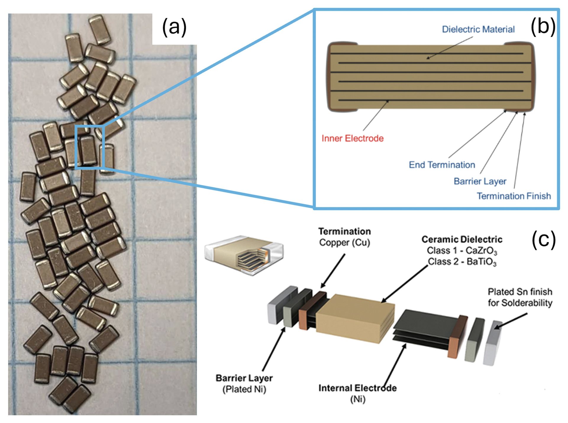
Multilayer ceramic capacitors (MLCCs) are one of the most common passive components (Figure 1a). MLCCs serve various roles in electronic packaging, including as energy storage devices, transient energy suppliers, and noise filters for electromagnetic signals. In general, MLCCs consist of dielectric (electrically insulating) materials placed between metal electrodes, typically nickel or silver-palladium alloys, in thin alternating layers (Figure 1b). These electrodes are connected on opposite sides of a metal termination layer (Figure 1c).

READ MORE
There are two main classes of dielectrics used in MLCCs. Class I or “linear” dielectrics are stable and reliable over a wide temperature range but store less energy per volume. Class II or “nonlinear” dielectrics store more energy per volume but have a smaller operating temperature range and are less stable. BaTiO3, which undergoes a phase transition from the ferroelectric to paraelectric phase at 125°C, is a Class II dielectric.1 This phase transition limits the operating temperature range for BaTiO3-based MLCCs, but it remains the preferred dielectric in hybrid integrated circuits due to the need for high volumetric efficiency.
MLCCs are produced by a co-firing process. First, nanoscale ceramic powder is mixed with a plasticizer and binder to form a slurry, which is then tape cast and dried into a large sheet. Next, metal electrodes are screen printed onto these sheets, which are then stacked, laminated, and cut into shape. Following burnout of the binder at about 400°C, the MLCCs are co-fired at about 1,200°C, which densifies and fuses the dielectric and electrode layer. Finally, metal termination layers are applied.
MLCC technology has advanced the miniaturization trend by reducing layer thickness to less than a micron and increasing the number of layers to hundreds, achieving typical dimensions of about 0.02 inches by 0.01 inches. But while decreasing layer thickness enhances capacitive volumetric efficiency, it poses challenges to reliability. Heightened electric fields within the thinner layers accelerates diffusion of oxygen vacancies to the ceramic–electrode interface, causing degradation.2 For this reason, MLCCs account for about 30% of failures in hybrid integrated circuits.
Finding a balance between volumetric efficiency and reliability requires advances in manufacturing and particle design. Manufacturing advances include fast firing in the initial co-firing step, which reduces interface roughness and differences in a layer’s thickness. A second firing step at a lower temperature and higher oxygen partial pressure oxidizes the BaTiO3–metal interface, which moves oxygen vacancies away from the interface and into the BaTiO3 grains.
Regarding particle design, decreasing particle size results in smaller grains with more grain boundaries, which can act as barriers to the migration of oxygen vacancies and improve reliability. Compositional engineering can lower oxygen vacancy concentrations as well and improve the dielectric’s temperature stability.
New models and tests are also being developed to understand and predict the degradation behavior and lifetime of MLCCs. These methods, when paired with our knowledge of defect and crystal chemistry, further guide innovations in dielectric design.
Together, this partnership between modeling and experimentation will help guide development of next-generation MLCCs.
References
1 Kishi et al., “Base-metal electrode-multilayer ceramic capacitors: Past, present, and future perspectives,” Jpn. J. Appl. Phys. 2003, 42(1): 1–15.
2 C.A. Randall and P. Yousefian, “Fundamentals and practical dielectric implications of stoichiometry and chemical design in a high-performance ferroelectric oxide: BaTiO3,” J. Eur. Ceram. Soc. 2022, 42(4): 1445–1473.
About the author
Sevag Momjian is a Ph.D. candidate at The Pennsylvania State University in professor Clive Randall’s group. He studies the cold sintering of dielectrics materials and the mechanisms enabling such densification. Outside of school, he enjoys playing soccer, tennis, and cooking.
Figure 1. (a) Typical MLCCs used in hybrid integrated circuits.
(b) Schematic of basic MLCC with alternating electrode (gray) and dielectric (beige) layers.
(c) Structure and material makeup of an MLCC.
Credit: (a) Sevag Momjian; (b,c) KEMET Corporation
COLLAPSE ARTICLE ABOVE
ACerS Young Professionals Network
ACerS Young Professionals Network (YPN) aims to provide support, community, and leadership opportunities to members as they transition from students to successful professionals in the broader ceramics society. Learn more.
From experiment to digital-powered materials science: My transition from academia to research at Leonardo Labs
By Alessandro De Zanet
Materials research and digital technologies are extremely intertwined fields nowadays. On the one hand, advanced materials are core components of the state-of-the-art computing, communication, and sensing technologies that make our world go round. On the other hand, systems powered by artificial intelligence and high-performance computing architectures are enabling the rapid design, analysis, and upscaling of new materials.
The increasing importance of and reliance on computational tools to advanced materials research has been discussed in some previous Bulletin articles.1,2 The topic gained new relevance to me after I graduated with my Ph.D. and entered the workforce as a Research Fellow at Leonardo Labs in April 2023.
READ MORE
Leonardo Labs are extensions of Leonardo (Rome, Italy), a global player in the aerospace and defense sector. These technological hubs, which are spread across the entire Italian peninsula, create synergies with local research ecosystems and Leonardo manufacturing sites. They focus on the research and development of cutting-edge technologies in several research areas, including Materials Technologies, Quantum Technologies, and Applied Artificial Intelligence, to name a few.
I work in the Materials Technologies area at Leonardo Labs in Rome, Italy. In my role, I carry out research on adhesion technologies and ceramic materials, with a strong focus on the importance of digitalization at all stages of the product development process, from early stages to its release and often beyond.
Before joining Leonardo Labs, I conducted mainly experimental work for my Ph.D. research on nonoxide ceramic matrix composite joints. This research was interesting and allowed me to acquire a lot of materials knowledge and experimental skills, but I only had a small taste of everything that falls under the umbrella of computational tools.
In the fast-paced world of industry, however, relying only on experimental methods to identify and develop new materials and processes will not let you keep pace with your competitors. For this reason, I have dedicated myself to enriching my toolkit as an experimental researcher with new computational skills.
For instance, I am exploring the use of finite element analysis (FEA) to virtually assess dissimilar joints and coatings. I use existing data for model pre-validation and training, and then I use the model to determine the most promising solutions for real-world testing. To improve predictability of the FEA model, we follow an iterative process: compare virtual results with real experiment outcomes, adjust the model based on discrepancies, and refine through multiple cycles. This process of continuous validation and adjustment enhances the model’s accuracy, making our predictions more reliable over time.
Executing these simulations, however, requires a balance between achieving high accuracy and managing computational time demands. Fortunately, our organization benefits from access to a proprietary supercomputer named davinci-1.3 The davinci-1 supercomputer plays a pivotal role in our company’s ambitious strategy of achieving comprehensive digitalization and integration of artificial intelligence across all processes. Its computational abilities free us from the typical constraints of processing power, thus allowing us to perform extensive simulations involving complex models swiftly and without sacrificing accuracy.
Of course, even as I am dedicating myself to enriching my toolkit, it is impractical to master every skill. Fostering collaborations with experts from diverse backgrounds and expertise becomes essential, and fortunately Leonardo Labs is structured to allow for such cross-disciplinary collaborations, internally and externally.
As I continue to advance in my professional career, I look forward to the collaboration and upskilling opportunities that Leonardo Labs affords me. But I also want to note the importance of actively participating in international professional societies, such as ACerS. These societies allow for interaction with professionals from all sectors and to stay updated on the main trends in the world of ceramics and the broader materials research community.
References
1 De Guire, E. “Materials Genome Initiative 10 years later: An interview with James Warren,” ACerS Bulletin 2021, 100(5): 24–28.
2 De Guire, E. “Harnessing artificial intelligence and machine learning to design new glasses,” ACerS Bulletin 2022, 101(4): 18–21.
3 “Supercomputer davinci-1,” Leonardo. Accessed 1 April 2024.
About the author
Alessandro De Zanet is a Materials Research Fellow at Leonardo Labs (Rome, Italy). His research focuses on adhesion technologies and the development of innovative ceramic-based solutions to address materials challenges. He is co-chair of the ACerS Young Professionals Network. Beyond his professional pursuits, Alessandro is passionate about spending quality time with family and friends.